Finished reading? Continue your journey in Tech with these hand-picked guides and tutorials.
Boost your workflow with our browser-based tools
Share your expertise with our readers. TrueSolvers accepts in-depth, independently researched articles on technology, AI, and software development from qualified contributors.
TrueSolvers is an independent technology publisher with a professional editorial team. Every article is independently researched, sourced from primary documentation, and cross-checked before publication.
Four chips, four price points, one confusing product family. Qualcomm's 2026 lineup spans two manufacturing nodes and three distinct performance tiers — and the flagship Pro chip's real-world advantage hinges on a thermal feature the standard model may not even get. Here's how to match each tier to your actual needs.
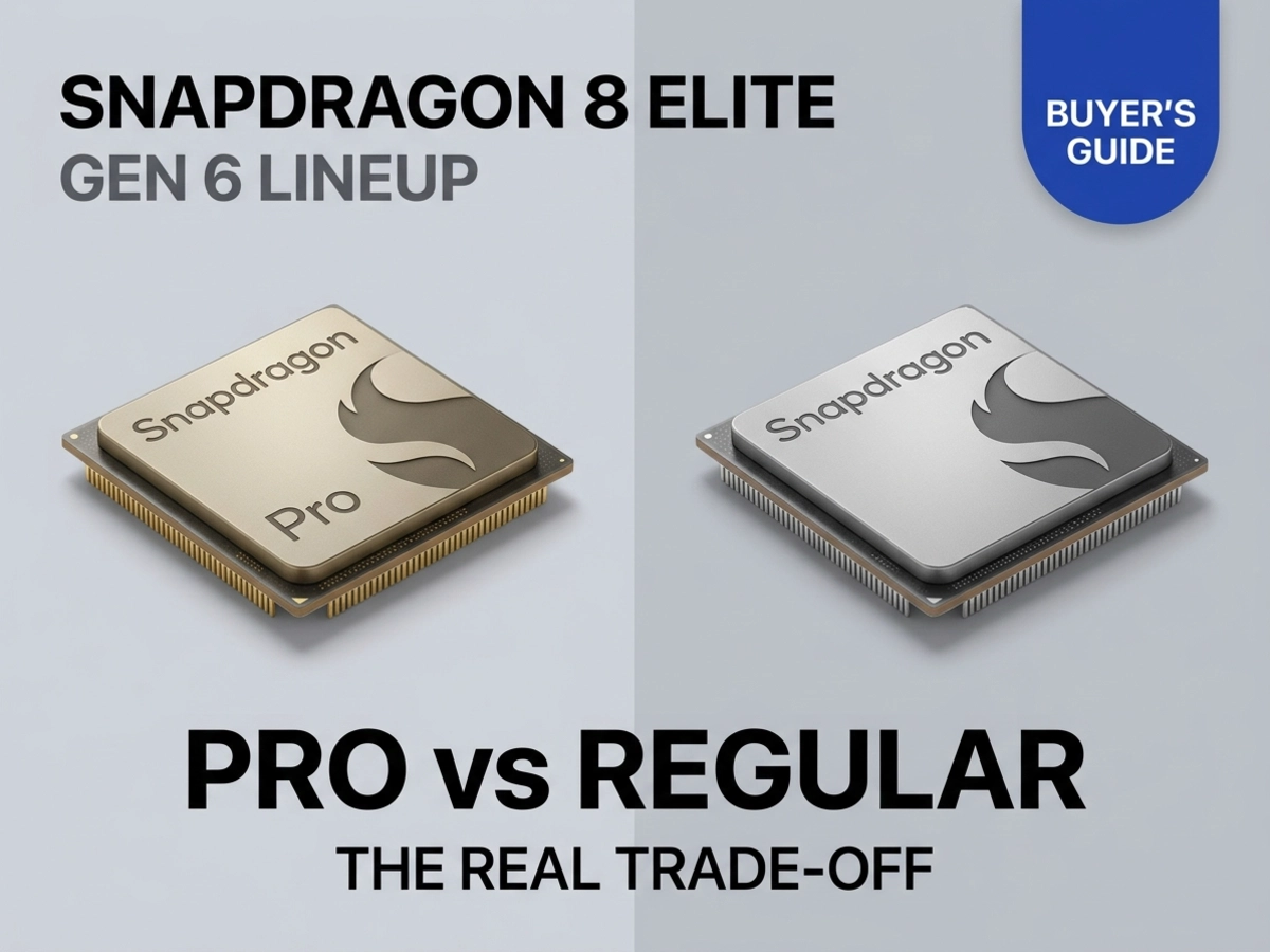
Late 2026 will bring the most fragmented Qualcomm chipset lineup in the company's history, and understanding it starts with a clear map of what exists.
At the top sits the Snapdragon 8 Elite Gen 6 Pro, model number SM8975. It pairs an Adreno 850 GPU with 18MB of GMEM (the GPU's dedicated on-chip rendering buffer) alongside a new 8MB last-level cache, and it brings LPDDR6 memory compatibility to the Snapdragon lineup for the first time. One level down is the standard Snapdragon 8 Elite Gen 6, model SM8950 — same 2nm manufacturing process, same 2+3+3 CPU core layout, but trimmed to an Adreno 845 with 12MB GMEM and a 6MB last-level cache, paired with LPDDR5X. Both 2nm chips use TSMC's N2P process node, which enters volume production in the second half of 2026 and delivers 5–10% better performance and power efficiency compared to the base N2 node it builds on. TSMC's N2 itself represented a 10–15% performance improvement over the previous 3nm N3E process, so these chips mark a genuine generational step in silicon efficiency.
Below the two new 2nm options, Qualcomm is expected to retain the Snapdragon 8 Elite Gen 5 from 2025 — repositioned at a lower price point as the 3nm option offering proven flagship performance without the cost premium of new silicon. At the bottom of the premium stack sits a new chip carrying model number SM8845 Pro, likely branded either the Snapdragon 8 Gen 6 or Snapdragon 8 Gen 5 Pro. It runs on a 3nm all-big-core architecture and functions as a modest step above the existing 8 Gen 5 — a cost-conscious option for brands building premium-tier phones that don't need cutting-edge process technology.
This four-tier structure mirrors the kind of CPU segmentation that desktop makers have used for years, but it marks a departure from Qualcomm's traditional single-flagship-per-cycle approach. Understanding why the company made this shift requires looking at what the specs actually mean — and at the economics that forced the decision.
The CPU architecture in the Pro and standard Gen 6 is identical: the same 2+3+3 Oryon core layout, built on the same N2P process. What separates these two chips is almost entirely in the GPU and memory subsystems — and those differences produce measurable gaps in specific workloads.
The GMEM difference deserves more attention than it typically gets. Adreno GPUs use a tile-based rendering approach where each frame is split into sections and rendered one tile at a time, with intermediate data held in the GMEM buffer rather than pushed back to system memory. Keeping that data on-chip is faster and reduces the load on the main memory bus. A larger GMEM buffer lets the GPU handle bigger tiles without spilling data to slower memory — and the Pro's 18MB versus the standard's 12MB represents a 50% increase in this on-chip capacity. That translates directly to frame consistency in demanding 3D scenes, ray tracing pipelines, and on-device AI inference tasks that require holding large data structures on-chip simultaneously. For gaming at high frame rates or running local language models, the gap shows up not just in peak benchmark scores but in how stable the output stays over time.
The memory standard is where the purchase decision gets complicated. Synopsys's technical documentation confirms that LPDDR6 reaches a maximum data rate of 14.4 Gbps versus LPDDR5X's ceiling of 10.67 Gbps, and that the new standard effectively doubles the available bandwidth per package through its 24-bit subchannel architecture. For memory-bound workloads — loading large AI models into active memory, processing high-resolution photo bursts, sustained gaming at maximum detail settings — that bandwidth increase is the headroom that prevents bottlenecks from forming.
The catch is cost. AndroidHeadlines reported that LPDDR6 runs approximately 20% more expensive than LPDDR5X and will initially ship only in 16GB configurations. That premium matters because the Pro chip technically supports LPDDR5X and even LPDDR5 as fallback options — meaning a manufacturer can build a Pro-branded phone using older, cheaper memory. Two devices both marketed as carrying the Pro chipset can deliver meaningfully different memory bandwidth depending on the configuration each manufacturer chose. Checking a specific phone's memory spec, not just its chip name, is the only way to confirm which setup you're actually getting.
Beebom's direct benchmark comparison of the 8 Elite Gen 5 (on the iQOO 15) and the cheaper 8 Gen 5 (on the OnePlus 15R) produced a result that reframes how to evaluate the entire Gen 6 tier structure. The 8 Elite Gen 5 peaked approximately 27% higher in 3DMark Wild Life Extreme burst testing than the lower-tier chip — that advantage is real and shows up in photography processing, brief gaming sessions, and AI tasks that complete in seconds. But under a 15-minute sustained CPU stress test, the Elite Gen 5 fell to 58% of its peak performance while the 8 Gen 5 held at 70%. In the GPU stress test, the gap was more dramatic: the flagship collapsed to 25% stability while the budget chip maintained 62.3%.
The 8 Elite Gen 5 throttled to just 58% stability under sustained CPU load on the iQOO 15 while the cheaper 8 Gen 5 held 70% — and in GPU stress testing the flagship collapsed to 25% stability while the budget chip held 62.3%. What this pattern reveals is that raw specification superiority at launch does not predict real-world sustained performance in a standard phone chassis. The cooling system of the device matters as much as the chip's theoretical ceiling — and the Gen 6 strategy is built around this lesson.
The Gen 6 Pro is expected to address this directly with an HPB (Heat Pass Block) thermal interface — a layer positioned between the chip package and the phone's vapor chamber that accelerates heat transfer before it reaches the cooling system. Samsung used a comparable architecture in the Exynos 2600. Combined with peak clock speeds reportedly reaching up to 5 GHz, the HPB is the engineering response to the throttling problem the Gen 5 exposed. Whether the standard Gen 6 will include HPB remains uncertain in pre-announcement leaks — which is precisely what makes the Pro's cooling system more significant than any individual GPU spec.
For users who primarily browse, stream, and shoot photos, sustained throttling is effectively invisible — those tasks don't run the GPU hard enough or long enough to hit thermal limits. For users who game at demanding settings for extended sessions, or who run on-device AI models continuously, the Pro's thermal architecture becomes the most consequential spec on the sheet — more important, in practice, than GPU model number or GMEM count.
Two independent cost pressures are hitting Qualcomm's handset business simultaneously, and it is their intersection — not either one alone — that explains why four chipset tiers became necessary.
The chipmaking side: TSMC's N2P node requires approximately $30,000 per wafer — nearly double the cost of current 3nm production. The Snapdragon 8 Elite Gen 5 was already priced at approximately $280 per unit, which was the most expensive mainstream chipset Qualcomm had offered at that point. The Pro is expected to exceed $300 per unit. When the processor alone consumes nearly a third of a phone manufacturer's total production budget for a high-end device, not every brand making a "flagship" phone can absorb that cost and still deliver a product that sells at competitive retail prices. The 2nm premium doesn't just make the Pro expensive — it creates a hard ceiling on how many OEMs can justify it for anything other than their top-tier SKUs.
The memory side is simultaneously severe. TrendForce's Q1 2026 pricing survey documented LPDDR5X contract prices surging approximately 90% quarter-over-quarter — the steepest quarterly increase in the standard's history — while NAND Flash contract prices are projected to rise 70–75% QoQ through Q2 2026. The underlying driver is a structural reallocation, not a cyclical shortage. Samsung, SK Hynix, and Micron — the three firms controlling over 95% of global DRAM production — have systematically shifted capacity toward high-bandwidth memory for AI accelerators, which generates three to five times the revenue per wafer that conventional LPDDR production earns. Gadget Hacks, citing supply chain data from Isaiah Research and PCSofter, reported that by Q1 2026 the combined cost of 16GB LPDDR5X RAM and 1TB UFS 4.1 storage had crossed $280 per device — exceeding the chip cost for the first time. Gadget Hacks, citing Isaiah Research, further reported Q2 Android supply chain DRAM pricing surging 80–90% QoQ. The overall smartphone bill of materials is rising roughly 25% due to memory costs alone. That increase lands on top of the chip premium, compounding the cost problem for every manufacturer building toward a specific retail price point.
Qualcomm's Q2 FY2026 Form 8-K specifies handset revenues of $6,024 million — a 13% year-over-year decline from $6,929 million in Q2 FY2025, with the company's Q3 guidance explicitly citing "memory supply constraints and related pricing on demand from several handset OEMs" as the primary headwind. Automotive revenue grew 38% in the same period and IoT grew 9%, but handsets remain the dominant revenue segment by a substantial margin. The earnings data confirms that the memory crisis is not a background condition — it is actively compressing Qualcomm's core business in real time.
Two cost crises are hitting Qualcomm's handset business simultaneously, and the fact that one is chipmaking-side while the other is memory-side is what makes the four-tier lineup an economic inevitability, not a marketing choice. A single 2nm flagship chip would force every OEM into the full Pro cost stack — chip premium plus memory premium plus margin pressure from the DRAM crisis, all at once. A retained 3nm option at a lower price lets manufacturers escape the wafer cost. Offering the standard Gen 6 alongside the Pro lets them access 2nm efficiency without the full GPU and memory cost of the top tier. Each tier in the lineup solves a specific combination of these two pressures, which is why a simple Pro/standard split was insufficient.
None of these specifications are officially confirmed; everything in this section is based on pre-announcement leaks that Qualcomm has yet to validate at Snapdragon Summit 2026. With that caveat in place, here is how each tier maps to a realistic buyer profile.
This chip belongs in a narrow category of devices: Ultra-branded phones from the top five Android OEMs, built with vapor chambers designed to take advantage of the HPB thermal system. The performance ceiling is genuinely higher — better sustained GPU output, LPDDR6 bandwidth for memory-hungry AI workloads, and peak clock speeds that matter for professional photography pipelines and extended gaming sessions at maximum detail. If the device is engineered around the Pro's thermal requirements and ships with LPDDR6 (which requires checking the memory spec, not just the chip name), it will justify the premium for power users running sustained workloads.
If the phone carries the Pro chip but ships with LPDDR5X — a configuration manufacturers can choose — the GPU advantage still exists, but the memory bandwidth story disappears. Verify the memory configuration before buying. It's worth noting that this kind of tiered chip differentiation isn't unique to Qualcomm: Apple's approach to binned chips in 2026 follows a structurally different logic that has direct consequences for how much the performance gap matters in practice — understanding both approaches helps when comparing platforms.
The volume chip for mainstream flagships in 2026 and early 2027. Same 2nm process as the Pro, same CPU architecture, meaningfully lower GPU and cache tier. For users who prioritize photography, everyday app performance, and periodic gaming at high but not maximum settings, this chip delivers the 2nm efficiency gains — better battery life at typical usage patterns, faster AI processing for on-device features — without requiring the cooling infrastructure or pricing premium of the Pro tier. Whether it includes HPB cooling is uncertain; buyers planning sustained gaming sessions should check OEM thermal specs for specific devices rather than relying on the chip model number alone.
The right choice for buyers who want a proven, mature 3nm flagship platform at a lower cost than new silicon. The Gen 5's performance is well-understood after a full launch cycle, its thermal behavior across different phone chassis is documented, and the devices built around it have been refined. The trade-off is a lack of the 2nm efficiency advantages that will show up in battery life under AI-heavy usage, and an older memory ecosystem at prices that are themselves now elevated by the DRAM crisis.
The option for brands building cost-conscious premium phones that need a flagship-adjacent chip without flagship-adjacent manufacturing costs. Performance exceeds the previous 8 Gen 5 in burst scenarios, and the 3nm all-big-core architecture keeps CPU-bound tasks competitive. GPU performance trails the Elite tier by a meaningful margin, and there is no path to LPDDR6 at this tier. For users who don't game at maximum settings or run sustained on-device AI workloads, this is a capable chip that lets manufacturers build well-rounded devices without the compound cost pressures of 2nm silicon and LPDDR6 memory.
The pattern across all four tiers is consistent: peak benchmark supremacy belongs to the Pro, but real-world sustained performance in a typical phone chassis depends on thermal engineering choices that the manufacturer — not Qualcomm — makes. Identify the use case, then check the thermal spec of the specific phone, not just the chip it carries.
Based on pre-launch leaks, the Pro chip (SM8975) is expected to appear primarily in Ultra-branded flagship devices from the top five Android OEMs — Xiaomi, Samsung, Oppo, Vivo, and OnePlus parent companies being the most likely candidates. AndroidHeadlines reported Xiaomi is already testing SM8975 hardware, though the company's final devices may not ship with LPDDR6 memory even if they carry the Pro chip. Samsung's Galaxy S27 Ultra is a natural candidate for the Pro tier if the Galaxy S series continues its recent pattern of using Qualcomm's top-tier chip. Volume flagship phones — the standard Galaxy S27, standard Xiaomi flagships, and mid-range premium offerings — are expected to use the standard Gen 6 or retained Gen 5 instead.
Qualcomm's Snapdragon Summit has consistently served as the announcement venue for its annual flagship mobile chipset. The 2025 Summit was held September 23–25 in Maui, Hawaii — a month earlier than the prior year's October event. A similar September 2026 timeframe is the most reasonable expectation for the Gen 6 announcement, with initial flagship phones following in October and November 2026. Nothing in this timing is officially confirmed, and Qualcomm has not announced a Summit 2026 date at the time of publication.
Not reliably. "Ultra" branding from major Android OEMs correlates strongly with the Pro chip tier — the economics of the Pro's cost premium make it impractical for anything below the Ultra category. But even within an "Ultra" device, the memory configuration (LPDDR6 versus LPDDR5X) is an OEM choice that won't necessarily appear in the product name. A phone marketed as an "Ultra" model with the Gen 6 Pro chip might still ship with LPDDR5X if the manufacturer decided the cost savings justified it. The only reliable way to confirm the full configuration is to check the device's official spec sheet for the memory standard, not just the chipset model.