Finished reading? Continue your journey in Tech with these hand-picked guides and tutorials.
Boost your workflow with our browser-based tools
Share your expertise with our readers. TrueSolvers accepts in-depth, independently researched articles on technology, AI, and software development from qualified contributors.
TrueSolvers is an independent technology publisher with a professional editorial team. Every article is independently researched, sourced from primary documentation, and cross-checked before publication.
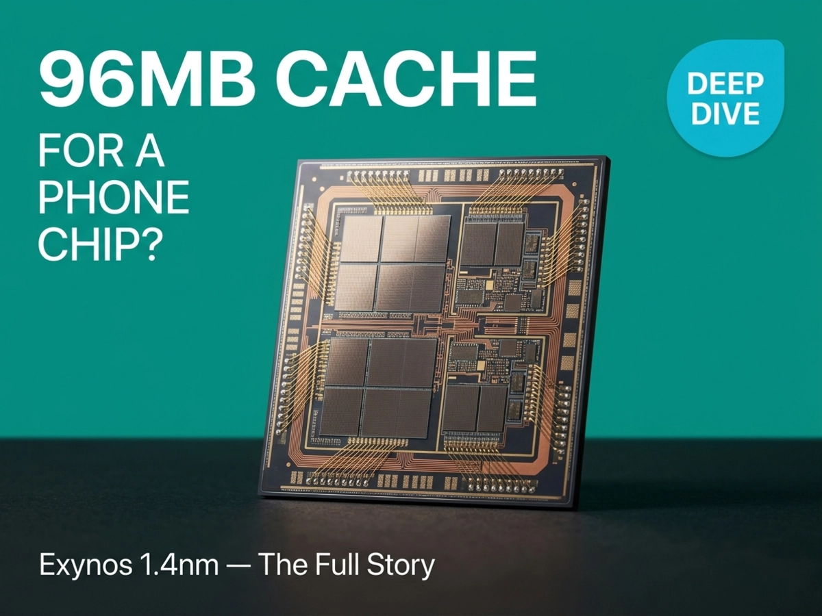
Samsung's 1.4nm Exynos leak includes a system-level cache of 96MB — nearly ten times the current smartphone maximum. The spec looks impossible for a phone chip, and it is. Understanding why requires separating two products sharing one architecture: a mobile chip for the Galaxy S28 and a Chromebook chip targeting Apple's M7. The distinction transforms what reads as engineering overreach into a coherent competitive strategy.
Modern mobile processors are heterogeneous computing systems — they contain CPU cores, GPU cores, neural processing units, and image signal processors all running simultaneously. Each of these blocks needs fast access to the same data, and routing every request all the way out to main memory is expensive in both time and power. System-level cache (SLC) solves this by placing a large shared pool of fast on-die memory between those compute blocks and the main DRAM sitting off the chip.
Unlike L1 and L2 caches, which are private to individual CPU cores, SLC is accessible to every compute unit on the chip at once. When the GPU finishes rendering a frame that the display engine needs, or the NPU produces inference results the CPU needs to act on, SLC allows that data handoff to happen on-chip rather than requiring a round-trip through external memory. The bigger the pool, the more working data the chip can keep accessible simultaneously — and the less frequently any individual block needs to wake the memory controller.
MediaTek's official Dimensity 9500 product page lists 10MB as its system-level cache — the highest figure currently in production smartphone silicon. The Exynos 2800 spec claims 96MB. That is not a marginal upgrade; it is a categorical jump into different territory.
The 96MB SLC figure doesn't describe a smartphone chip — it describes a Chromebook chip that also happens to run on a phone platform, and the distinction is what makes this specification technically coherent rather than absurd.
Tipster Schrödinger's leaks, as reported by Tweaktown, confirm that Samsung is preparing two separate variants of the Exynos 2800: a standard mobile chip for the Galaxy S28 flagship and a dedicated Chromebook chip targeting Apple's entry-level M7. The 96MB SLC and ultra-wide bus width are properties of the Chromebook variant, not the phone.
The reference point Samsung is calibrating against makes the figure immediately less surprising. Apple's M-series chips range from 8MB SLC in the base M4 up to 96MB in the highest-tier M-series configurations. Samsung's Chromebook variant is targeting the same cache tier that Apple uses for its most capable laptop silicon — direct competitive calibration, not spec-sheet inflation. Apple demonstrated the strategy's viability first: scale a phone-class chip architecture to laptops, share the underlying design investments across a wider product range, and compete in markets that previously required entirely separate silicon development programs. Samsung is following the same logic.
The implications for the phone variant remain genuinely unclear. Splitting the architecture into phone and laptop configurations almost certainly means the mobile Exynos 2800 ships with substantially less SLC — consistent with the physical reality explored next.
The reason 96MB can't fit comfortably in a smartphone chip has nothing to do with ambition and everything to do with memory circuit physics. Cache is built from SRAM — static random-access memory — which requires six transistors per stored bit, compared to one transistor and one capacitor for DRAM. That six-transistor structure is what makes SRAM fast enough to sit between the processor and the rest of the memory hierarchy, but it is also what makes SRAM intrinsically area-hungry on silicon.
The problem deepens at advanced process nodes. Logic transistors have scaled aggressively: each new node delivers more transistors per square millimeter for the compute circuitry. SRAM cells have not kept pace. Semiconductor Engineering reported that TSMC's 3nm node offered essentially no improvement in SRAM bit cell density over 5nm, a finding disclosed at the IEEE International Electron Devices Meeting in 2022. TSMC's 2nm GAA process partially revived SRAM scaling, but the gap between logic and SRAM density improvements has become a structural feature of advanced node economics.
The consequence is counterintuitive: adding more cache at a smaller process node is not cheaper or easier — it is proportionally more expensive, because the SRAM area needed grows as a fraction of total die area while the logic around it shrinks. Apple explicitly chose, with M5, to keep the die at roughly the same size as M4 rather than saving the space freed by denser logic transistors, and instead filled it with additional SRAM for a larger SLC. That is a deliberate choice trading die cost for performance — something a laptop chip, which commands a higher selling price per unit, can justify in a way a phone chip, packed tightly into a form-factor-constrained package, generally cannot.
Samsung's 1.4nm GAA process may improve SRAM density further through its four-nanosheet transistor architecture, but the structural constraint doesn't disappear. A 96MB SLC remains a laptop-class specification regardless of which node it's built on.
Samsung's 2nm foundry yields were still in the mid-50s% range as recently as April 2026, trailing TSMC's reported 60-70%, and Qualcomm had already redirected its next flagship SoC to TSMC's 2nm — yet Samsung's internal chip teams were already testing designs on the 1.4nm node.
TrendForce, citing Busan Ilbo, documented that Samsung's 2nm yields remain below the roughly 60% threshold considered stable for mass production. After backend processing and binning, effective yields fall further. Qualcomm's decision to take its Snapdragon 8 Elite 6th Gen to TSMC rather than Samsung is the clearest market signal of the gap. SammyGuru reported that Samsung officially pushed its 1.4nm mass production target from 2027 to 2029 at SAFE Forum 2025, with VP Shin Jong-shin citing the priority of stabilizing 2nm processes first. That delay put Samsung one year behind TSMC's own 2028 1.4nm target.
The most plausible reading of this timeline suggests Samsung is following the same foundry playbook it used to build GAA expertise in the first place. Its SF3E node in 2022 was the first commercial GAA process anywhere — years before TSMC and Intel adopted the architecture — and Samsung used its own Exynos chips as the primary customer for that process while external orders were scarce. The Exynos 2600, released in the Galaxy S26, was the first 2nm GAA chip in mass production anywhere. Now Samsung appears to be doing the same thing at 1.4nm: testing internal silicon on the node before commercial customers have committed, generating the process learning and telemetry that foundry customers will later need to see before signing contracts. Samsung confirmed in its Q1 2026 earnings that 1.4nm development "remains on track" for 2029. The Exynos 2800 testing is likely part of what "on track" means in practice.
These are early specifications from a single tipster, not confirmed Samsung disclosures. The gap between testing specifications and final shipping silicon is substantial, and the 1.4nm mass production timeline carries real uncertainty.
Early specifications for the 1.4nm Exynos include a 25% efficiency gain over 2nm — an unconfirmed figure from the same tipster disclosure, not an independently verified foundry target. The physical mechanism behind the claim is grounded in how the process is structured. Tom's Hardware, citing DigiTimes' reporting on Samsung VP Jeong Gi-Tae's disclosure, reported that SF1.4 will increase the number of nanosheets per transistor from three to four.
In gate-all-around architecture, each nanosheet is a thin horizontal silicon channel surrounded on all sides by the gate material. More nanosheets per transistor means more total channel area for current to flow through — improving the transistor's switching speed and drive current. Equally important, additional nanosheets give the gate better electrostatic control over the channel, reducing the leakage current that bleeds through even when the transistor is nominally switched off. That leakage reduction is where efficiency improvements at the process level originate: less wasted power per transistor compounds into meaningful differences at the chip level across billions of switching events per second.
Foundry-level PPA targets — the performance, power, and area metrics that Samsung publicly associates with each process node — describe what the transistor architecture is capable of under optimal conditions. They are not the same as what a finished chip delivers in a real device. The gap between the two depends on circuit design, thermal management, software stack maturity, and manufacturing consistency. Samsung's SF2P node carried efficiency improvement targets similar in scale, and the Exynos 2600, its first major chip on 2nm, still showed a real-world power efficiency deficit. TrendForce, citing Chosun Biz testing, found that the Exynos 2600 trails the Snapdragon 8 Elite Gen 5 by up to 28% in real-world battery life despite being manufactured on a newer process node.
The four-nanosheet mechanism is physically sound and represents a genuine architectural improvement over three-nanosheet designs. But Samsung's track record of translating foundry-level PPA targets into chip-level efficiency leadership is still being established. The 1.4nm efficiency claim should be read as a process target, not a delivered result — a meaningful distinction for anyone evaluating what the Exynos 2800 will actually do when it ships.
The Exynos 2800 leaks point to something beyond a node upgrade. AndroidHeadlines reported that Samsung is developing fully custom CPU cores for the Exynos 2800 — a return to in-house CPU design that would be Samsung's first since the Exynos 990 in 2020. The company disbanded its Austin CPU design team of roughly 290 engineers around 2019 after its Mongoose cores consistently underperformed ARM's off-the-shelf Cortex designs on thermal efficiency and battery life. The Exynos 990 was the last Mongoose chip.
Alongside the custom CPU return, Samsung is reportedly ending its AMD RDNA GPU collaboration — the Xclipse series that debuted with Exynos 2200 in 2022 — and replacing it with a fully in-house GPU architecture. The Chromebook variant's GPU (Xclipse 980) reportedly supports full path tracing, which simulates light interaction physically rather than using shortcuts, placing it in the same rendering capability tier as dedicated workstation graphics rather than mobile gaming chips.
Taken together — custom CPU, custom GPU, proprietary foundry process, cross-device platform strategy — the Exynos 2800 represents Samsung's attempt at the vertical integration model that gives Apple its competitive moat. The 96MB SLC in the Chromebook variant is one specification within that broader architecture, not an isolated headline. The Exynos 2600's real-world trade-offs — including that 28% battery deficit against Qualcomm — demonstrated precisely what Samsung needs to improve to make a fully custom chip competitive. The Exynos 2800's design choices — abandoning both AMD and ARM licensing — read as a direct structural response to that gap. Whether Samsung's custom architectures, developed without the institutional knowledge lost when the Mongoose team was shut down, succeed where the Mongoose generation failed is the question that will determine whether the 1.4nm specs become a product or remain an ambition.
The timeline has two reference points, and they don't fully align. Schrödinger's leaks, as reported by Tweaktown, indicate Samsung is targeting tape-out by the end of 2026, with the Galaxy S28 series as the planned launch vehicle in 2028. That would place the chip in commercial devices roughly two years before Samsung's stated 1.4nm mass production target of 2029.
The apparent gap reflects how chip development typically works: tape-out, validation, and limited production can begin before a node achieves the yields required for full commercial mass production. Samsung's Q1 2026 earnings confirmed 1.4nm development remains on track. The more meaningful uncertainty is whether the Chromebook variant follows the mobile launch immediately or arrives on a separate timeline — no confirmed schedule exists for the laptop product.
Almost certainly yes, though not at 96MB. The current Exynos 2600 features 16MB of SLC — already a step above the 10MB maximum in current shipping smartphone silicon. The 96MB figure is tied specifically to the Chromebook variant, where die area economics and price points can absorb the SRAM cost.
A mobile Exynos 2800 built on 1.4nm would likely see meaningful SLC expansion compared to the 2600 — Samsung has consistently grown cache capacity across Exynos generations. Apple's own mobile chips operate in a progressively larger SLC range at each generation, which is a reasonable reference trajectory for what a competitive flagship mobile chip on 1.4nm might follow. The exact figure for the mobile variant remains unconfirmed.