Finished reading? Continue your journey in Tech with these hand-picked guides and tutorials.
Boost your workflow with our browser-based tools
Share your expertise with our readers. TrueSolvers accepts in-depth, independently researched articles on technology, AI, and software development from qualified contributors.
TrueSolvers is an independent technology publisher with a professional editorial team. Every article is independently researched, sourced from primary documentation, and cross-checked before publication.
Apple's Baltra chip has been covered as a server hardware story. It's actually a three-stage dependency-reduction plan — one that explains why Apple reserved more advanced chip packaging capacity at TSMC than AMD's entire AI portfolio, and what that means for the company's long-term AI ambitions.
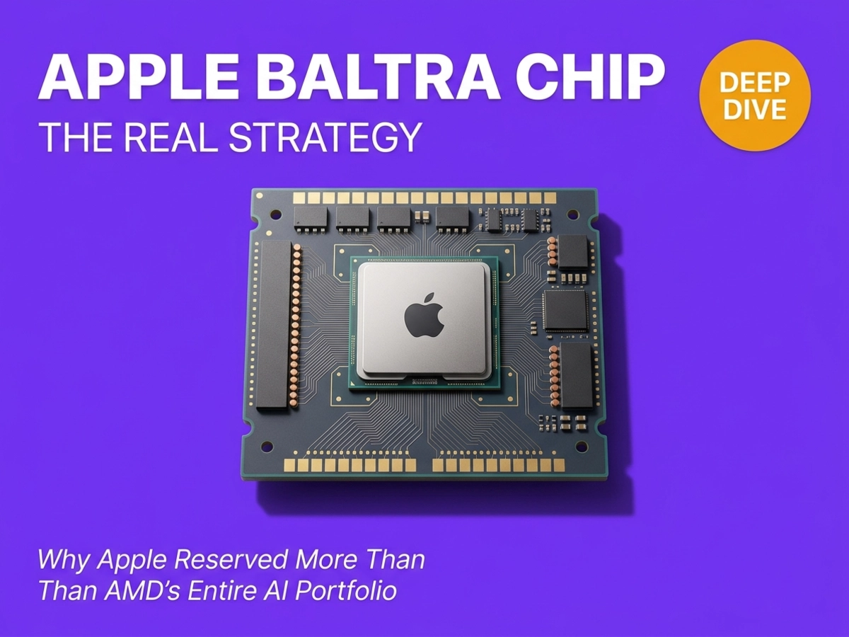
Apple is building its first purpose-designed AI server chip, codenamed Baltra. Unlike the M-series chips it repurposed for server use when Apple Intelligence launched, Baltra is an application-specific integrated circuit built exclusively for running AI inference in Apple's data centers — not for selling computers or training models. Broadcom is Apple's design partner specifically for the chip-to-chip networking layer, the high-speed communication fabric that allows multiple processors to function as a coordinated cluster. The chip targets TSMC's second-generation 3nm N3E manufacturing process and is expected to use a modular, chiplet-based architecture where each die handles a distinct function.
To understand why any of that matters, the best starting point is a pair of numbers. Investing.com, citing Morgan Stanley analyst Erik Woodring's analysis, reports that Apple has placed orders for TSMC's advanced SoIC packaging capacity equivalent to 36,000 wafers for 2026 and 60,000 wafers for 2027. SoIC — System on Integrated Chips — is TSMC's 3D stacking technology, the method that allows separate dies to be bonded directly on top of one another rather than placed side by side on a flat substrate.
Apple's Mac product line can justify at most 1,600 SoIC wafers annually — and Apple reserved 36,000 of them for 2026.
The gap is not a rounding error. Investing.com, citing Morgan Stanley analyst Erik Woodring, puts the Mac figure at approximately 1,600 wafers — the combined SoIC demand for M-series Pro, Max, and Ultra chips at Apple's actual shipping volumes. The same analysis notes that AMD, currently TSMC's largest SoIC customer, will consume around 42,000 wafers in 2026. Apple's 36,000 reservation for the same year puts it within striking distance of AMD's entire SoIC consumption — and its 60,000-wafer commitment for 2027 would substantially exceed it.
Morgan Stanley's analyst attributed the bulk of Apple's reserved capacity to Baltra, describing the chip as Apple's move to replace existing M-series servers used for Private Cloud Compute with purpose-built AI inference silicon. He also noted candidly that performance and efficiency at scale remain "key unknowns" — which means Apple is committing to enormous foundry capacity for a chip whose production results haven't yet been validated. That exposure isn't reckless; it reflects a calculated bet that controlling packaging allocation now is worth more than waiting for validated performance data.
That last detail is the tell. Apple is not simply ordering wafers because it has calculated exactly how many Baltra chips it will need by Q3 2027. It is pre-booking TSMC's SoIC priority customer tier before the competition peaks. SemiAnalysis documents that as Apple scales its M5 and M6 Ultra chips using advanced packaging, its requirements begin converging on the same packaging lines that NVIDIA uses — specifically AP6 and AP7 in TSMC's facility network. Apple and NVIDIA historically competed for entirely different packaging infrastructure. That separation is ending, and the company reserving capacity earliest stands at the front of the queue when allocation decisions are made.
Apple's early, aggressive reservation is a hedge against the capacity pressure that arrives when that competition becomes direct. Morgan Stanley characterizes Apple's infrastructure spending as more likely capex than opex — a structure that fits the 18-to-24-month break-even math that custom AI silicon generates at scale. The foundry reservation is, in that sense, a capital investment in queue position as much as it is a production order.
Understanding why Baltra's SoIC adoption matters requires understanding what the technology actually changes about how chips are built. The relevant distinction is between two methods of stacking dies on top of each other.
In conventional face-to-back stacking, the two dies are oriented so that signals must travel through the base die's through-silicon vias — small vertical conductors that pierce the chip — before reaching the top die. Through-silicon vias introduce latency, add energy overhead, and cannot be packed at fine pitch across active transistor regions without affecting density. TSMC's North American Technology Symposium presentation specifies that face-to-face SoIC bonding achieves 14,000 signals per square millimeter, roughly 9× the density of face-to-back stacking, which achieves approximately 1,500 signals per square millimeter in real-world designs. Face-to-face bonding aligns the metal layers of two dies directly, creating copper-to-copper connections so short and dense that communication between stacked dies approaches the behavior of on-chip wiring.
TSMC reached a 6-micron pitch in 2025 and is targeting 4.5 microns by 2029, meaning Baltra's 2027 deployment window lands exactly when 3nm TSV technology is expected to mature, enabling the most advanced process nodes to be stacked on top of each other. For chip designers, this is what makes SoIC the successor to transistor-level scaling: when shrinking individual transistors yields diminishing returns, stacking them more densely in three dimensions becomes the next lever for increasing compute per watt.
For Baltra, the chiplet architecture means multiple specialized dies handle different tasks — AI computation, networking, I/O — rather than combining every function into a single monolithic design. Each chiplet can be optimized for its specific role. The performance case for this approach is straightforward. The strategic case is less discussed.
The chiplet segmentation that gives each Baltra die a discrete function also solves a problem Apple has not stated publicly: it means Broadcom, Apple's design partner for the interconnect layer, can see individual chiplets but never the assembled architecture.
tttechnology.co.uk reports that Broadcom receives chiplet-level access during design, not system-level visibility. That boundary preserves Apple's intellectual property from the partner it depends on to build the chip. This matters because Broadcom occupies an unusual structural position in the AI infrastructure market. Together with Marvell, the company enables more than 80% of hyperscaler custom AI silicon. Broadcom's design relationships span Google's TPU, Meta's MTIA, Microsoft's Maia, and now Apple's Baltra simultaneously. That breadth gives Broadcom enormous leverage — and creates an inherent tension for every company that uses its services. Apple's chiplet segmentation is the architectural answer to that tension: work with Broadcom for what you cannot yet build yourself, while ensuring Broadcom cannot see what you are ultimately building.
The performance optimization and the IP protection are not two separate decisions. They are a single architecture serving both goals at once.
Baltra is an inference chip. It will not train models, and Apple has shown no indication of building training infrastructure at the scale Google or Amazon operate. That scope is sometimes described in coverage as a limitation. It is the opposite.
Apple's Private Cloud Compute security research documentation confirms the system was built exclusively on Apple Silicon from launch. The PCC architecture provides three security properties — stateless computation (data is wiped after each request), verifiable transparency (security researchers can inspect system behavior), and non-targetability (requests cannot be directed to specific nodes) — that are only enforceable when Apple controls the hardware completely. A chip from NVIDIA or any other external vendor cannot be incorporated into PCC without undermining the privacy promise that PCC exists to deliver. Baltra is not an optional upgrade to the server infrastructure. It is the eventual endpoint that PCC's architecture requires.
Apple has been building toward this endpoint in stages. The company originally deployed M2 Ultra chips in its Private Cloud Compute servers — consumer silicon pressed into data center service — then jumped directly to M5-based servers, skipping the M3 and M4 generations that were widely discussed as upgrades. That Houston, Texas facility, built with Foxconn, entered production in October 2025, ahead of schedule, and represents the current bridge between repurposed consumer chips and the purpose-built Baltra generation. For readers evaluating how the M5 chip itself performs across different compute workloads, the chip's capabilities relative to competing platforms like Snapdragon X2 and Intel Panther Lake are mapped in detail here.
The economics reinforce the same conclusion from a different angle. Training a model is a capital expense: it happens once, or a small number of times, for any given model generation. Inference is an operating expense that scales with every user query, every response, every interaction across Apple's 2 billion active devices. Custom ASICs built for inference typically reach break-even against GPU procurement in 18 to 24 months at hyperscale volumes, then compound savings for the rest of the chip generation's lifespan. Futurum Group survey data reported by Data Center Knowledge found that in 2025, GPUs represented 58% of data center compute spending, but in 2026, custom accelerators are projected to lead growth at 22%, ahead of GPUs at 19%.
The cost case at scale is concrete. Introl Blog, citing The Information's reporting, documented that Midjourney cut its monthly compute bill from $2.1 million to $700,000 — a 65% reduction — by migrating inference workloads from NVIDIA GPUs to Google TPUs. Midjourney's workload is repetitive, architecturally stable, and optimized for throughput. Apple's inference workload for Apple Intelligence carries the same profile: a defined model architecture, predictable query patterns, and a scale that makes per-query economics decisive.
An inference-only chip built for PCC satisfies both the privacy requirement and the financial requirement simultaneously. Neither consideration alone would fully explain the design choice. Together, they make Baltra's narrow focus the only rational architecture.
Glass substrates are the next-generation replacement for the organic (plastic-based) materials currently used in flip-chip ball grid array packages — the base layer on which dies are mounted. They enable finer circuit traces, better thermal stability, and potentially 30% or more reduction in power consumption relative to organic alternatives. Samsung Electro-Mechanics has been developing this technology at its pilot production facility in Sejong, South Korea, targeting mass production after 2027.
What makes Apple's engagement with Samsung Electro-Mechanics unusual is the specific way it is structured. SammyGuru, citing The Elec's reporting, confirmed that Samsung Electro-Mechanics has been providing glass substrate samples to Apple independently since at least 2025. The same technology is being sampled to Broadcom separately. Two parallel evaluation streams, for the same material, from two parties who work together.
MacObserver reports that Baltra mass production begins in the second half of 2026, with server deployment in 2027. Samsung Electro-Mechanics targets glass substrate mass production after 2027 — which is exactly when Apple would be evaluating substrate choices for the generation of chips that follows Baltra. Apple is running this evaluation now, on its own timeline, developing independent technical judgment about a material whose production window aligns with its next design cycle.
Samsung Electro-Mechanics is sampling the same glass substrate technology to Apple and to Broadcom — separately.
The only strategic reason to evaluate the same packaging material independently from a partner who is also evaluating it is to avoid depending on that partner's technical conclusions about the material. Broadcom handles the interconnect and networking layer of Baltra — the portion of chip design most directly shaped by substrate properties. A company deferring entirely to Broadcom on substrate evaluation would be handing Broadcom judgment over a technology that determines how much of Baltra's successor architecture Broadcom will be needed to design. This alignment is consistent with Apple building the option to eventually redesign the packaging layer without depending on Broadcom's judgment — though Apple may simply be conducting independent technology due diligence rather than executing a planned exit. What is certain is that Apple is building the technical understanding it would need to make that choice.
The wafer reservation, the chiplet segmentation, and the Samsung SEMCO independent evaluation each look, in isolation, like reasonable engineering decisions for a company entering the AI server business. Viewed together, they describe something more deliberate.
The wafer reservation secures Apple's position as TSMC's highest-priority SoIC customer before Baltra's production peaks — using capital commitment now to guarantee access when packaging demand from NVIDIA and AMD converges on the same lines. The chiplet architecture allows Apple to work with Broadcom for the interconnect capabilities it cannot yet build internally, while ensuring no partner sees the full design. The independent glass substrate evaluation builds the technical judgment Apple would need to eventually reduce Broadcom's role in a future generation.
Each move makes sense on its own. But the sequence — capacity first, then IP isolation, then packaging knowledge acquisition — describes a company that is not just building a chip. It is constructing the infrastructure for full-stack AI compute ownership: the kind that Apple's Private Cloud Compute architecture has demanded from the beginning, and that only becomes achievable once Apple controls every layer from silicon to inference.
Two genuine uncertainties remain. Baltra's actual inference performance at scale has not been validated, and Morgan Stanley's analyst was explicit that this is an open question. And whether Apple can bring packaging design in-house before needing to negotiate a renewed Broadcom engagement remains unknown — the Samsung SEMCO glass substrate work is at sampling stage only, not production readiness. Apple is building toward a particular destination. The speed at which it arrives depends on execution at layers that haven't shipped yet.