Finished reading? Continue your journey in Tech with these hand-picked guides and tutorials.
Boost your workflow with our browser-based tools
Share your expertise with our readers. TrueSolvers accepts in-depth, independently researched articles on technology, AI, and software development from qualified contributors.
TrueSolvers is an independent technology publisher with a professional editorial team. Every article is independently researched, sourced from primary documentation, and cross-checked before publication.
The 5GHz smartphone chip milestone is real, and it is almost entirely a TSMC foundry achievement rather than a CPU design breakthrough. But peak speeds rarely survive contact with a real phone chassis: the current 4.6 GHz generation already throttles below 60% within minutes. Here is what that means for every flagship launching in 2026.
Each successive semiconductor process node delivers three compounding advantages: smaller transistors, higher switching speeds, and lower power consumption per operation. Those gains allow chips to run at higher clock speeds without exceeding the power budget that keeps a phone's battery alive, and the 5GHz milestone arriving in 2026 traces directly to one specific transition in the manufacturing roadmap.
TSMC's 2nm node (N2) entered volume production in Q4 2025, as TSMC's official 2nm technology page confirms. The node introduces a transistor architecture called gate-all-around (GAA) nanosheet technology for the first time in TSMC's production lineup. In a GAA transistor, the gate electrode surrounds the current channel on all four sides rather than three, which improves electrical control and reduces leakage current at small dimensions. This is the foundational shift that enables the performance gains the 2nm family promises.
The base N2 node delivers up to 15% faster operation at the same power consumption and 25–30% lower power consumption at the same speed, compared with the N3E process that powered many 2024-era chips. But the variant that matters most for the 5GHz milestone is N2P, an enhanced iteration of N2 scheduled for high-volume manufacturing in the second half of 2026. According to Futurum Research, N2P delivers up to 18% better performance at identical power and approximately 36% lower power at the same speed versus N3E, with a 1.2x increase in transistor density.
TSMC's 2nm technology page specifies that N2 volume production started in Q4 2025 as planned, with nanosheet transistors delivering full-node improvements in performance and power. Both Qualcomm and MediaTek have committed to N2P rather than the base N2 node for their next-generation flagship chips, with mass production targets in late 2026. MediaTek's Dimensity 9600 series is among the first mobile designs publicly confirmed to target that node.
That 18% frequency headroom is the number that matters most. The current generation of TSMC 3nm chips peaks around 4.26 to 4.6 GHz. Add 8 to 10 percent of that figure and you land at 5GHz. The process node delivers that increment. The chipmakers capture it.
Within a single process generation, chip architecture creates meaningful performance differences. The A19 Pro and the Snapdragon 8 Elite Gen 5 both run on the same TSMC N3P node and produce significantly different clock speeds and efficiency profiles — which reveals how chipmakers are competing inside the headroom their foundry partner provides.
Qualcomm's Snapdragon 8 Elite Gen 5, introduced in September 2025, runs its two prime cores at up to 4.6 GHz on TSMC's N3P process. The chip uses Qualcomm's third-generation Oryon CPU, which for the first time shares its architecture with the Snapdragon X Elite line used in Windows laptops. Qualcomm claims 20% better CPU performance and 35% improved power efficiency versus the previous generation. The Samsung Galaxy S26 variant runs its prime cores at 4.74 GHz, the highest clock speed in any commercial smartphone as of early 2026.
Apple's A19 Pro takes a different approach to the same node. Performance cores run at up to 4.26 GHz, lower than Qualcomm's flagship, but Apple's chip achieves single-core Geekbench 6 scores that outperform both AMD's Ryzen 9 9950X and Apple's own M4. The explanation lies in instructions-per-clock: Apple's CPU microarchitecture executes more work per cycle, making raw frequency a less decisive variable. Apple's documentation confirms the A19 Pro delivers up to 40% better sustained performance than the A18 Pro when paired with the iPhone 17 Pro's vapor chamber cooling system.
Apple's iPhone 17 Pro technical specifications page confirms the A19 Pro performance cores run at up to 4.26 GHz on TSMC's N3P process, a figure that reflects Apple's deliberate choice to prioritize instructions-per-clock efficiency over headline frequency.
MediaTek's Dimensity 9500 currently sits between the two in clock terms, with a peak prime core at 4.21 GHz on N3P. The next generation, the Dimensity 9600 series, targets near-5GHz on N2P, with the Pro variant adopting a dual-prime-core configuration rather than the single-prime-core design of the Dimensity 9500. That architectural shift — and whether it translates to genuine competitive parity with Qualcomm's equivalent generation rather than just matching its cluster count — is explored in depth in Why Dimensity 9600's Dual-Core Design Is More Than a Spec Match.
The architecture choices visible in today's chips explain why the A19 Pro can outperform the faster-clocked Snapdragon in single-threaded workloads while running at a lower frequency. But the gap between any of these chips and the 5GHz threshold requires a new process node, not a new CPU design.
The Snapdragon 8 Elite Gen 5 runs at 4.6 GHz on TSMC's N3P node; the next generation targeting 5GHz shifts to N2P, an 18% faster and 36% more efficient process, a ratio that makes the foundry transition, not the chipmaker's architecture team, the primary driver of frequency headroom in the 2026 generation. Qualcomm and MediaTek chose N2P specifically because N2P enables the frequency ceiling that reaches 5GHz; the architecture teams are optimizing within the headroom the node provides, not creating headroom independently.
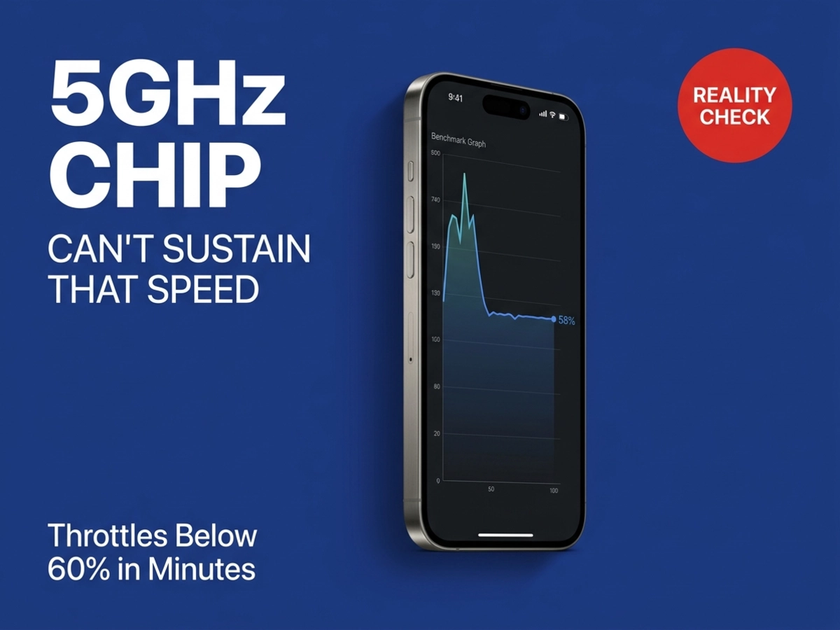
Benchmark numbers are measured at a chip's fastest sustainable speed, which is not the same as the speed it maintains during a prolonged gaming session, an AI video processing task, or a long rendering job. The gap between those two figures is where the 5GHz story gets complicated.
Beebom's 15-minute CPU throttling test on the Snapdragon 8 Elite Gen 5, conducted on the iQOO 15, shows the chip maintaining peak speed for approximately 3 minutes before dropping to 58% of peak performance for the remainder of the test. The GPU tells a similar story: in 3DMark's Wild Life Extreme Stress Test, the Adreno 840 posted a peak loop score and then settled at 25% stability by the 20th round.
PhoneArena's testing on the Nubia Z80 Ultra, a conventionally cooled flagship, found the phone achieving 48% stability in the same 3DMark stress test, with a final loop score of 3,064. That number sits below what the previous-generation Snapdragon 8 Elite achieved in the Honor Magic V5 (4,443 points) and even below the Xiaomi 14 Ultra's Snapdragon 8 Gen 3 score of 4,018. Internal chip temperatures in the Nubia reached above 50°C under sustained load.
The contrast with purpose-built gaming hardware is significant. The RedMagic 11 Pro, equipped with a massive vapor chamber, a nano ceramic liquid pump, and an active cooling fan spinning at 24,000 RPM, maintained 80% stability in the same test conditions. That device achieves what its mainstream counterparts cannot: it keeps temperatures low enough to sustain near-peak clocks. But it does so through a thermal solution that most phone buyers never choose.
The point is not that the Snapdragon 8 Elite Gen 5 is a flawed chip. It posts peak scores that represent the fastest sustained burst performance available in any Android device. The point is that the chip's headline frequency describes what it does for the first few minutes, not what it does during the workload a buyer is actually performing.
The Snapdragon 8 Elite Gen 5 is simultaneously the fastest smartphone chip and, in most real-world devices, a chip that cannot sustain its fastest speeds for more than a few minutes; a contradiction that the 2026 generation will inherit unless phone makers solve the cooling challenge that chip engineers cannot.
The physics driving this are structural. A vapor chamber, which is the standard cooling technology in flagships from Apple, Samsung, and Qualcomm's partners, works by moving heat away from the chip hotspot and distributing it across the device's chassis. A working fluid evaporates at the hotspot, travels to cooler regions, condenses, and returns. This is substantially more effective than a solid metal spreader. But the chassis itself is the final heat sink, and a phone's chassis has a fixed, small surface area.
XDA Developers' thermal analysis specifies that vapor chambers work by distributing heat across the chassis rather than expelling it from the device, meaning that once the chassis itself reaches thermal capacity, no further improvement in internal heat spreading changes the outcome.
Once the chassis reaches saturation, the chip throttles. A larger vapor chamber delays that point, which is why the iPhone 17 Pro's new aluminum unibody vapor chamber improves sustained performance markedly over the iPhone 16 Pro's thermal solution. But it does not eliminate the underlying constraint.
Sustained AI workloads amplify this problem beyond what gaming does. A three-minute burst of gaming has natural rest periods; a 15-minute on-device transcription or real-time translation task does not. The era of on-device AI is arriving precisely as the flagship chips most capable of running those models are hitting the limits of what passive cooling can sustain.
The only current solution that changes the constraint rather than extending how long it takes to hit it is active cooling: a fan that moves air across a heat exchanger. Gaming phones implement this; mainstream flagships do not, because their buyers prioritize thinness and silence. Testing by PhoneArena confirmed this divide directly: the RedMagic 11 Pro with its active cooling fan maintained 80% stress-test stability, while the conventionally cooled Nubia Z80 Ultra dropped to 48%. For the 5GHz generation arriving in late 2026, that gap will be even more consequential.
The Huawei narrative in most coverage treats the company's chip situation as a simple node-generation deficit: TSMC makes 3nm chips, SMIC makes 7nm chips, and the gap is obvious. The actual situation is more precise than that, and the precise version reveals why Huawei's performance gap persists even as SMIC has made genuine technical progress.
SMIC's N+3 process node, used in the Kirin 9030 that powers the Huawei Mate 80 series launched in November 2025, was analyzed by Canadian research firm TechInsights. The Kirin 9030 is SMIC's first commercial chip built on N+3, its most advanced node, and SMIC cannot use EUV (extreme ultraviolet) lithography to manufacture it. ASML's EUV machines are blocked under US export controls. Instead, SMIC uses older DUV (deep ultraviolet) equipment at 193nm wavelength, applying the same feature up to four times per layer using a technique called multi-patterning to achieve fine-enough circuit dimensions.
TechInsights' analysis of the Kirin 9030, as documented by PhoneArena, confirms the N+3 process achieves roughly 125 million transistors per square millimeter, a figure that demonstrates SMIC's progress is real and greater than the clock speed comparison alone would suggest.
TechInsights confirms the Kirin 9030 achieves roughly 125 million transistors per square millimeter, matching Samsung's 5LPE node density, yet its prime core still tops out at 2.75 GHz. The data points toward SMIC's DUV-imposed interconnect limitation as the binding frequency constraint, rather than any deficit in transistor count itself: density and clock frequency are not the same engineering outcome, and SMIC's multi-patterning process appears to be the ceiling that keeps Kirin clocks far below those of TSMC-manufactured chips despite the narrowing transistor count gap.
The reason deserves explanation. Transistor density describes how many switching elements fit in a given chip area. Clock frequency describes how fast those elements switch. Switching speed depends critically on how narrow and low-resistance the metal wires connecting transistors can be made. Those wires are manufactured by the same patterning process, and with DUV multi-patterning, each successive exposure step introduces small positional errors that accumulate. The result is a minimum reliably manufacturable metal line width that is wider than what EUV can achieve, which means greater resistance, which caps the maximum clock frequency at which the circuit can operate without excessive leakage and heat.
SMIC has achieved Samsung 5LPE-equivalent transistor density. The Kirin 9030's Geekbench 6 single-core score of 1,131 and multi-core score of 4,277 reflect not a transistor count problem but this interconnect ceiling, placing the chip's raw compute output in the range of a mid-range Android device from 2023 despite the genuine manufacturing achievement the N+3 node represents.
The yield question introduces an additional uncertainty. Exact yield rates for SMIC's N+3 node are disputed, with industry estimates ranging from below 20% to as high as 60–70% depending on chip complexity and workload type; SMIC has not disclosed official figures. Better yields would reduce per-chip cost and improve supply reliability. They would not change the frequency ceiling imposed by DUV's interconnect limitation, which is a physics constraint rather than a manufacturing quality constraint.
The foundry picture shapes not just which phones perform better but also what those phones cost and how long their peak-spec experience actually lasts.
TSMC commands 70.2% of global foundry revenue as of Q2 2025, a record high measured by TrendForce. Samsung holds roughly 7% and SMIC around 5%. Advanced nodes — 7nm and below — account for the majority of TSMC's revenue. No other foundry can absorb large-volume orders for leading-edge chips with competitive yield rates, which means Apple, Qualcomm, and MediaTek have no realistic alternative for their flagship silicon. TSMC's pricing reflects that position.
Counterpoint Research estimates TSMC's N2 wafers at approximately $30,000 per wafer, a roughly 30% premium over N3 wafer costs. TSMC's price increase notification to customers, reported by Tom's Hardware, confirms 5–10% hikes across all sub-5nm nodes starting January 2026, a cost structure shift that compounds with the N2 wafer's already elevated pricing at approximately $30,000 per wafer. Chipmakers build wafer costs into chip pricing, and phone makers build chip costs into device pricing. Flagship phones with 2nm chips in late 2026 will cost more to manufacture than their 3nm predecessors.
The Samsung Exynos 2600 offers a useful calibration point. Samsung markets it as the world's first 2nm smartphone chipset, and it powers the Galaxy S26 in certain regional markets. Its peak CPU core runs at 3.8 GHz — lower than the Snapdragon 8 Elite Gen 5 at 4.6 GHz on 3nm. This reflects Samsung's 2nm yields, which remained below 50% as of late 2025, and the different optimization choices Samsung made in its process. Node number and clock frequency are not a simple one-to-one relationship; TSMC's 3nm N3P produces higher peak frequencies than Samsung's 2nm SF2 node because TSMC's process maturity and design ecosystem are further along.
For a practical buyer framework, the following considerations now carry more weight than they did in the 3nm era.
First, the foundry determines the performance floor. Phones running TSMC-manufactured chips — all iPhone 17 variants, Galaxy S26 in Snapdragon regions, OnePlus, Xiaomi, and most global flagship Android devices — occupy a performance tier separated from Huawei's Kirin-based devices by a gap that cannot be closed through software optimization or camera upgrades.
Second, the phone's thermal design determines the performance ceiling. Two phones carrying an identical chip will deliver meaningfully different sustained performance depending on whether the device has a large vapor chamber, active fan cooling, or relies solely on graphite sheets. Spec sheets do not disclose sustained performance under load. Stress test reviews from outlets that publish 15-minute throttling test results are the most useful buying signal for anyone who plans to use demanding apps consistently.
Third, 2nm chip phones in late 2026 will carry a premium. The 5GHz generation is real and achievable, but the cost to manufacture those chips is substantially higher than today's 3nm alternatives. Buyers who want the headline performance should anticipate paying more for it.
Fourth, the 5GHz number on a spec sheet describes burst performance. Whether a specific device can approach that frequency under sustained load depends on cooling design, not chip generation. The RedMagic 11 Pro's active cooling achieves 80% stress-test stability with today's 4.6 GHz chip; most mainstream flagships achieve 25–48% with the same silicon. The same bifurcation will exist for 5GHz devices.
Yes. The Exynos 2600 demonstrates exactly this point. Samsung's chip runs on its SF2 2nm process with a peak CPU core at 3.8 GHz, compared to the Snapdragon 8 Elite Gen 5 at 4.6 GHz on TSMC's 3nm N3P process. In that comparison, the older node from the better-executing foundry produces a higher peak frequency.
The reason is process maturity and design rule optimization. TSMC's N3P benefits from more advanced yield techniques, better-characterized design rules, and a longer production ramp than Samsung's newer SF2. Samsung's 2nm node yields remained below 50% as of late 2025, which affects not only cost but also how aggressively the chip can be clocked without defects causing failures. TSMC's equivalent yield on its 3nm node is substantially higher, allowing more aggressive frequency binning.
The practical takeaway: node generation names from different foundries are not directly comparable. "2nm" from Samsung is a meaningfully different manufacturing environment than "2nm" from TSMC. Chip performance correlates more reliably with which foundry made the chip than with the node number on the spec sheet.
For buyers within China who prioritize Huawei's software ecosystem, camera hardware, or specific connectivity features, the Kirin 9030-powered Mate 80 series is a genuine product with real capabilities. The chip represents genuine engineering achievement on SMIC's part.
For buyers evaluating raw processing performance, the Kirin 9030's Geekbench 6 single-core score of 1,131 and multi-core score of 4,277 position it closer to a 2022–2023 mid-range Android chip than to current TSMC-manufactured flagships. The prime core's 2.75 GHz ceiling is not primarily a chip design failure but a consequence of DUV lithography's interconnect limitations that SMIC cannot circumvent without EUV equipment.
A buyer who needs maximum performance for gaming, video editing, or on-device AI workloads will find the gap between Kirin 9030 and a Snapdragon 8 Elite Gen 5 device substantial in practice. A buyer whose needs center on communication, photography, and standard app use will find the Kirin 9030 adequate, with the caveat that the software ecosystem on Huawei's HarmonyOS differs materially from the Android and iOS ecosystems in terms of third-party app availability outside China.
Precise device pricing depends on how phone makers absorb or pass through higher component costs, so no specific retail figure can be stated with certainty. What the foundry economics do make clear is the direction and magnitude of the cost pressure.
Counterpoint Research estimates TSMC's N2 wafer pricing at approximately $30,000 per wafer, a roughly 30% premium over 3nm wafer costs. TSMC compounded that pressure by notifying customers of 5–10% price hikes across all sub-5nm nodes starting January 2026. When a chipmaker pays more per wafer and receives more good dies, the cost per good chip may not increase proportionally, but when premium node adoption is new and yields are still ramping, per-chip costs rise.
Flagship phones launching in H2 2026 with Snapdragon 8 Elite Gen 6 Pro or Dimensity 9600 Pro on N2P should be expected to carry a meaningful premium over their 3nm predecessors. Buyers who want 5GHz performance at 3nm prices will likely need to wait until N2P yields have matured and competitive pressure has normalized pricing, which historically happens 12 to 18 months after a new node's first commercial launch.
Specifications for the Snapdragon 8 Elite Gen 6, Dimensity 9600 Pro, and Apple A20 referenced in this article represent leaked or rumored information as of early April 2026. Qualcomm, MediaTek, and Apple have not confirmed final specifications for those products.