Finished reading? Continue your journey in Tech with these hand-picked guides and tutorials.
Share your expertise with our readers. TrueSolvers accepts in-depth, independently researched articles on technology, AI, and software development from qualified contributors.
TrueSolvers is an independent technology publisher with a professional editorial team. Every article is independently researched, sourced from primary documentation, and cross-checked before publication.
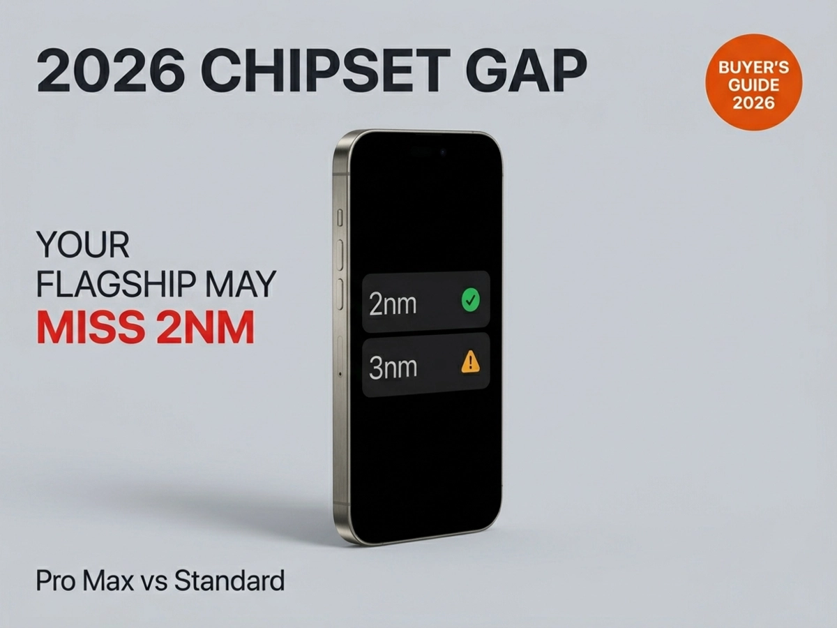
Paying for a flagship smartphone in late 2026 no longer guarantees the best chipset — TSMC's 2nm supply crunch is forcing Apple, Qualcomm, and MediaTek to reserve their most advanced silicon for Ultra and Pro Max models only. This guide breaks down which phones get the top chip, what you lose if yours doesn't, and how to choose your next upgrade.
Apple reserved more than half of TSMC's initial 2nm output before Qualcomm or MediaTek had finalized their designs — and that single allocation decision is the force behind every dual-chipset announcement you will see in late 2026.
The supply math is unforgiving. TSMC's CEO stated publicly in November 2025 that the company's advanced-node capacity falls roughly three times short of what customers are demanding. That shortfall spans 5nm, 3nm, and the incoming 2nm node simultaneously. What makes 2nm particularly constrained is that AI chip demand and smartphone SoC demand are now pulling from the same fabrication pool, with Nvidia, AMD, and cloud infrastructure providers competing for the same wafer slots as phone chipset designers. None of TSMC's newer international facilities — the fabs under construction in the United States, Japan, and Europe — are yet delivering high-volume 2nm output, so every 2nm wafer in 2026 comes from two plants on the island of Taiwan.
Those two plants are fully booked through 2026, with monthly output targeting 100,000 wafers by year-end. Initial capacity started at just 40,000 wafers per month. To put that into context, each 2nm wafer costs approximately $30,000 compared to roughly $20,000 for a 3nm wafer — about 50% more expensive — and each wafer produces only 300 to 400 chips. The economics naturally filter 2nm access to customers who both need and can afford the premium, and who moved early enough to secure an allocation.
Apple qualifies on both counts and moved decisively. WCCFTech, citing DigiTimes reporting, documented that Apple secured more than half of TSMC's initial 2nm production capacity, a move that keeps rivals from matching its access to leading-edge silicon ahead of the iPhone 18 launch. Apple accounted for 24% of TSMC's total revenue in 2024, making this a customer relationship TSMC has every incentive to prioritize. With Apple's allocation consuming the majority and AI chip orders from Nvidia, AMD, and others absorbing much of what remains, Qualcomm and MediaTek are working within genuinely tight windows. Neither company can order enough 2nm wafers to put their best possible chip in every premium Android device. Their response — splitting each flagship lineup into a Pro variant for ultra-premium models and a standard variant for the broader market — is an adaptation to that constraint, not a product philosophy choice.
The chipset tier split follows a consistent pattern across every major platform: the most powerful 2nm processor goes to the top-tier model in each manufacturer's lineup, and the standard flagship slots in just below it.
On the Apple side, the A20 Pro will power the iPhone 18 Pro, iPhone 18 Pro Max, and iPhone Fold at their expected September 2026 launch. The base A20 chip is slated for the standard iPhone 18, which Apple has restructured into a 2027 release under a new split-launch schedule. For buyers who want the full A20 Pro experience, the iPhone 18 Pro is the entry point — choosing the base iPhone 18e or waiting for the standard model means landing on a different generation of silicon entirely.
The Android picture follows the same logic. Qualcomm's Snapdragon 8 Elite Gen 6 Pro is expected to carry pricing exceeding $300 per unit, which limits its appearance to a small number of ultra-premium devices. This dual-chipset structure is not new territory for the industry — it mirrors the Pro/standard split Apple has used for years with its A-series chips, and Qualcomm's decision to follow the same architecture reflects the same underlying reality: limited top-tier silicon, channeled to the products that can support the highest retail prices. The standard Snapdragon 8 Elite Gen 6 will power the broader flagship market; it skips LPDDR6 memory support to remain competitively priced.
MediaTek is following the same playbook. The Dimensity 9600 Pro includes LPDDR6 memory, UFS 5.0 storage, and ARM's Magni GPU, while the standard Dimensity 9600 runs on LPDDR5X and UFS 4.0. MediaTek is expected to reveal the full lineup around September 2026, targeting Asian OEMs — Vivo and Oppo are among the likely early adopters for the Pro variant in their top-of-range products. The standard chip will be more accessible for brands competing on price.
The practical rule for buyers is straightforward: if a phone's model name does not include "Ultra," "Pro Max," or an equivalent top-tier designation, there is a real chance it is running the standard chipset variant, not the Pro.
The tier gap is not about raw clock speed. It is about three specific platform features that all Pro chipsets share and all standard variants give up: GPU tier, memory type, and storage interface.
Qualcomm's leaked specifications confirm the split clearly. The Pro model (SM8975) carries an Adreno 850 GPU with 18MB of graphics memory (GMEM) and full LPDDR6 support. The standard model (SM8950) steps down to an Adreno 845 with 12MB GMEM and tops out at LPDDR5X. Both chips use a 2+3+3 CPU core architecture, so the processing cores themselves are similar — but the GPU and memory subsystem are not.
Qualcomm's Pro variant gets an Adreno 850 GPU and LPDDR6 memory while the standard variant receives an Adreno 845 and LPDDR5X; MediaTek's 9600 Pro gets the Magni GPU, LPDDR6, and UFS 5.0 while the non-Pro stays on LPDDR5X and UFS 4.0 — the feature delta is identical across both companies. That convergence is not coincidence. GPU compute and memory bandwidth are exactly what benefits most from a 2nm fabrication process at full production volume. When supply is constrained, chipmakers reserve those gains for the tier that can justify the higher wafer cost.
Those differences show up in real workloads. On-device AI inference, gaming frame rates at high graphical settings, and video encoding throughput all depend heavily on GPU performance and the bandwidth ceiling that memory type creates. LPDDR6 offers meaningfully higher peak bandwidth than LPDDR5X; UFS 5.0 storage roughly doubles sequential read speeds compared to UFS 4.0. The Pro tier is not paying for a faster name badge — it is paying for a wider data pipeline throughout the chip.
Early engineering samples of the Dimensity 9600 Pro have registered Geekbench 6 single-core scores of 4,200–4,300 and multi-core scores of 12,000–12,500. These figures come from pre-production samples, which routinely score above what commercial units achieve, so the final retail performance may land somewhat lower. A separate thermal caveat applies: the dual 5GHz performance cores are expected to throttle to approximately 4GHz under sustained load, which can narrow the gap in long-running tasks like extended gaming sessions.
The 2nm supply crunch does not operate in isolation. A simultaneous global memory shortage is driving up component costs across every price tier — and its effects are harshest on the buyers who were already priced out of the Ultra tier.
The root cause is structural. Samsung, SK Hynix, and Micron — the three manufacturers that supply the vast majority of the world's DRAM — have shifted significant cleanroom capacity toward high-bandwidth memory (HBM) for AI data centers. HBM earns considerably higher margins than standard consumer-grade DRAM, making the reallocation a straightforward business decision for each manufacturer. Every wafer dedicated to HBM for an AI accelerator is a wafer not available for the LPDDR modules inside a smartphone. New capacity from SK Hynix's M15X facility and Micron's Idaho fabs is expected to come online across 2026 and 2027, but meaningful price relief for consumer DRAM is not anticipated before 2028. The result for smartphone buyers: DRAM prices have roughly doubled since early 2025, with no near-term reversal in sight.
IDC's February 2026 blog on the global memory shortage specifies that memory represents 15-20% of the bill of materials for mid-range smartphones, and projects smartphone build costs rising 10-25% across tier segments by the end of 2026. For a phone in the $300–$500 range where margins are already thin, a cost increase of that magnitude is difficult to absorb without raising prices or trimming specifications — both of which are already occurring across the industry.
FoneArena, citing Counterpoint Research data, reported that global smartphone SoC shipments are projected to fall 7% in 2026 even as SoC revenues grow double digits — fewer phones sold at higher revenue per phone tells the story of an industry consolidating upward and leaving the mid-range behind. Counterpoint also projects the average smartphone selling price to rise 6.9% year-on-year in 2026, a figure that reflects rising memory costs flowing directly through to retail prices.
The 2nm crunch and DRAM shortage look like the same crisis from a distance, but they hit buyers in opposite directions depending on what tier of phone they are shopping for. If you are buying an Ultra or Pro Max, the chipset gap is real and the premium is at least partially justified by genuinely better silicon — faster GPU, wider memory bandwidth, higher-throughput storage. If you are buying a standard flagship or a mid-range device, you are paying more than last year's equivalent phone offered, often for specs that have stagnated or been quietly trimmed. The industry is moving upward; the value proposition at $300–$500 is shrinking.
Understanding the supply mechanics leads directly to a practical conclusion: do not expect 2nm chipset costs to fall meaningfully within the next 12 months, and plan your upgrade accordingly.
TechSpot reported that TSMC's 2nm wafers are priced at approximately $30,000 each — around 50% more than 3nm wafers, and TSMC has reportedly implemented a no-discount policy for its 2nm customers. With the two domestic 2nm plants sold out through 2026, there is no supply glut on the horizon that would force prices down. Counterpoint Research documents TSMC holding roughly 87% of the sub-5nm smartphone SoC production market, which means there is no competing foundry capable of providing relief at scale. The pricing structure this year reflects a durable floor, not a launch-year premium that fades.
Samsung's Exynos 2600 — technically the world's first commercially shipped 2nm GAA smartphone chip — demonstrates why it is not a viable alternative route. GizmoChina's testing documented peak power draw of 30W for the Exynos 2600 compared to 21W for the Snapdragon 8 Elite Gen 5 — a roughly 40% disadvantage that undercuts the efficiency promise of 2nm entirely. Samsung's foundry yields also lag behind TSMC's, and the device performance results confirm that gap has real consequences. Qualcomm and MediaTek have no reason to shift volume orders to Samsung under these conditions.
With the supply picture unlikely to shift before 2027, buyers face a concrete set of options:
If sustained AI performance and premium gaming matter: An Ultra or Pro Max device with a confirmed 2nm Pro chipset is the only path to the full platform advantage — faster GPU, LPDDR6 memory, UFS 5.0 storage. XiaomiToday reported the Snapdragon 8 Elite Gen 6 Pro is expected to exceed $300 per unit, which will translate to Ultra-tier retail pricing. The premium is real, but so is the differentiation.
If those workloads are secondary: The standard Snapdragon 8 Elite Gen 6 and standard Dimensity 9600 will still be 2nm-class chips — capable, efficient, and faster than their 3nm predecessors. They skip LPDDR6 and the top-tier GPU, but for everyday productivity, photography, and casual gaming, the performance gap will not be noticeable in daily use. The question of whether chipset tier gaps translate to real-world differences is not new — a scenario-based comparison of current-generation flagship chips shows that the same pattern holds today: for casual users, both tiers feel fast enough; the gap only surfaces under sustained workloads and emulation. The risk in the standard tier is paying inflation-adjusted prices for a chip positioned deliberately below the top.
If budget is the primary constraint: Current-generation 3nm flagships — the Snapdragon 8 Elite Gen 5, Dimensity 9500, and Apple A19 Pro — are still genuinely powerful chips. A mid-cycle purchase at a discounted price on today's 3nm hardware may offer better value-per-dollar than a 2026 mid-range device running higher-cost components that constrain its own specifications. The DRAM shortage is pricing mid-range phones upward; bargain-hunting on proven 3nm silicon is a rational counter-move.
Counterpoint forecasts that 2nm will remain confined to flagship and premium products for at least two to three years. The pressure on standard and mid-range prices is not seasonal. Buyers who choose a tier should do so with the understanding that the chipset gap they are accepting in 2026 is likely to remain a feature of the market through 2028 at minimum.
Not for the phones most buyers are considering. Samsung's Exynos 2600 is the first commercially shipped 2nm GAA smartphone chip, but it is exclusively used in Samsung's own Galaxy S26 series in select markets — it is not available to Qualcomm or MediaTek, and neither company has signaled interest in Samsung's foundry for their flagship SoCs.
The performance data further diminishes the appeal. Testing documented by GizmoChina found the Exynos 2600 drawing approximately 30W at peak, compared to 21W for Qualcomm's current Snapdragon 8 Elite Gen 5. That roughly 40% power disadvantage directly undermines the efficiency case for switching to 2nm. Samsung's foundry yields also lag behind TSMC's — Samsung reached approximately 50% yield by early 2026, while TSMC was operating at 65–70% — and lower yields mean higher effective cost per good chip. Until Samsung closes both the yield and efficiency gaps, its 2nm process cannot serve as a genuine relief valve for the broader market's supply constraints.
Counterpoint Research documents TSMC controlling approximately 87% of sub-5nm smartphone SoC production, a figure that reflects years of customer concentration rather than a temporary condition. A meaningful shift in that balance would require Samsung to demonstrate sustained yield parity and efficiency competitiveness — neither of which appears imminent for 2026.
The most realistic timeline is 2028 or later. Counterpoint Research forecasts 2nm adoption remaining limited to flagship and premium products for at least two to three years from initial production, meaning mid-range and standard flagship devices are unlikely to see full 2nm feature access before late 2028. TSMC's own capacity roadmap targets 200,000 wafers per month by 2028 — when production volume rises to that level, the cost dynamics will shift and broader adoption becomes economically viable.
The DRAM shortage adds a second constraint beyond chipsets. Android Authority reported DRAM prices roughly doubling since early 2025, with supply relief unlikely before 2028 as new capacity from SK Hynix's M15X facility and Micron's Idaho fabs comes online across 2026 and 2027. Standard flagship phones that might otherwise benefit from 2nm-era efficiency gains will continue to face higher memory costs that compress their specifications even if chipset access eventually broadens.
For buyers deciding between waiting and buying now: the 2026–2027 window is not likely to reward waiting for standard phones to close the Pro gap. The supply math and pricing structure are both durable. The more useful question is whether the Pro-tier features — LPDDR6, UFS 5.0, top-tier GPU — matter for the specific workloads on the device. For most daily use cases, the answer is probably no, which makes a well-positioned current-generation 3nm flagship a reasonable alternative to paying Ultra-tier prices for the full 2nm platform.