Finished reading? Continue your journey in Tech with these hand-picked guides and tutorials.
Share your expertise with our readers. TrueSolvers accepts in-depth, independently researched articles on technology, AI, and software development from qualified contributors.
TrueSolvers is an independent technology publisher with a professional editorial team. Every article is independently researched, sourced from primary documentation, and cross-checked before publication.
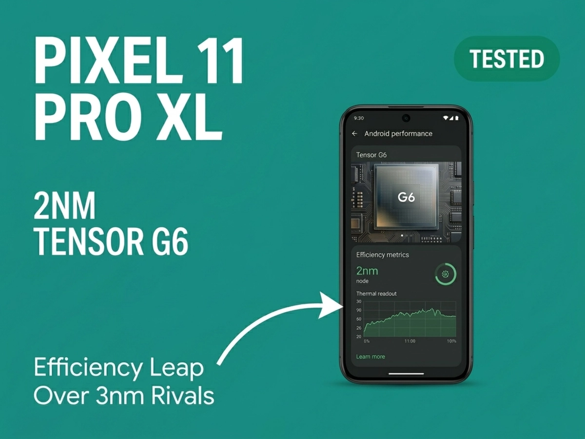
Google's Pixel 11 Pro XL arrives with manufacturing technology that finally matches the industry's cutting edge. The Tensor G6 processor uses TSMC's 2-nanometer process while competitors still ship 3nm chips, and this node advantage combines with MediaTek's M90 modem to create genuine efficiency gains. For buyers deciding whether to wait or purchase current flagships, understanding these technical improvements reveals how Google addresses its historical thermal weakness.
Internal Google engineering documents identify thermal complaints as the leading driver of Pixel phone returns, accounting for 28% of all user satisfaction mentions and those same documents acknowledge that the device's thermal comfort thresholds were set too high and needed to be lowered, along with plans for a Cinematic Rendering Engine in the Tensor G6 designed to cut power consumption during video recording by roughly 40%.
Previous Tensor generations addressed heat through software, not hardware. When the processor approached thermal limits, the operating system reduced clock speeds through adaptive throttling. This kept device temperatures within acceptable bounds, but it did so by trading performance away. Users who ran intensive tasks noticed the device becoming warm and then slowing down. The heat was not being prevented; it was being managed after the fact by doing less work.
Each software mitigation bought time without solving the underlying cause. The Tensor G6 takes a different approach entirely. Rather than managing heat once it is generated, the chip reduces how much heat is generated in the first place, through three hardware-level changes made simultaneously.
The central claim of the Tensor G6 is a 2nm manufacturing process from TSMC. Understanding what that means requires separating the marketing shorthand from the physics.
TSMC confirmed that its N2 process entered high-volume manufacturing in Q4 2025, making it available for consumer device launches in the first half of 2026. This matters for credibility: the Pixel 11's expected August 2026 window follows the production ramp by roughly eight months, which is consistent with the lead time chip designers need for finished consumer silicon.
The performance gains from N2 are substantial. At the 2024 International Electron Devices Meeting, TSMC disclosed that N2 achieves a 24–35% reduction in power consumption at the same operating voltage, or up to 15% higher performance at the same power level, compared to its 3nm technology. A reduction of that magnitude at equivalent clock speeds is not a rounding error in chip design terms. Less power consumed means less heat generated, directly. The relationship is physical, not speculative.
The reason N2 achieves these gains is architectural, not merely cosmetic. Every prior TSMC process node used FinFET transistors, which wrap the gate around three sides of the channel. N2 moves to nanosheet Gate-All-Around architecture, where the gate surrounds the channel on all four sides. This fuller enclosure gives the transistor better electrostatic control, which reduces the current that leaks through when the transistor is nominally switched off. That leakage current is wasted energy converted directly to heat. Reducing it cuts both power draw and thermal output simultaneously.
The Snapdragon 8 Elite Gen 5 powering the Galaxy S26 Ultra uses TSMC's N3P process. N3P is a performance-optimized revision of 3nm FinFET, offering incremental gains over the original N3E but it remains FinFET architecture. It does not use Gate-All-Around transistors. Adjacent node numbers imply incremental separation. These chips use fundamentally different transistor architectures, and the efficiency gap between N3P and N2 is wider than that framing suggests.
Process node improvements address the processor's power consumption. But the cellular modem runs independently, and it runs continuously whenever a phone has a signal. On any smartphone, the radio subsystem is one of the largest continuous power draws, operating in parallel with everything else the device does.
Multiple supply chain reports, including coverage from 9to5Google, indicate that Google is testing the MediaTek M90 for integration with the Tensor G6. MediaTek announced the M90 at Mobile World Congress 2025. The M90 documentation confirms a 12 Gbps peak downlink rating, dual 5G SIM dual-active support, and laboratory testing that achieved 11.6 Gbps under simultaneous sub-6GHz and millimeter-wave connectivity and its UltraSave technology reduces average modem power consumption by up to 18% compared to the prior generation. The modem also incorporates an AI layer that analyzes active data traffic patterns and device context in real time, selecting the most power-efficient combination of carrier frequencies for a given situation.
Consumer chip comparisons tend to focus on SoC die temperature in isolation, but modem-sourced heat is a consistently underweighted factor. During a video call, a 4K upload, or extended streaming, the modem and processor run simultaneously at elevated loads. Both generate heat into the same physical chassis. An 18% efficiency gain from the modem does not add linearly to the 2nm chip gains; it compounds them, because peak device temperatures during intensive tasks reflect both heat sources running at once.
The Tensor G6's 2nm node is the foundation. A 24–35% reduction in power consumption at the same operating voltage means the chip's primary heat output drops substantially from the Tensor G5 baseline. This applies continuously: every computation, every background process, every on-chip AI inference operation runs through transistors that waste less energy as heat than the previous generation.
The M90 modem's 18% average power reduction eliminates a significant parallel heat source. Prior Pixel thermal complaints were not exclusively about the processor; sustained cellular activity was a compounding factor. By pairing the Tensor G6 with a modem that runs cooler during typical use, Google removes heat contribution from a subsystem that processor-focused thermal analysis routinely ignores.
The Tensor G6 integrates a new Titan M3 security chip, the first major refresh to Google's dedicated security silicon since the Titan M2 debuted with the Pixel 6 in 2021. The Titan M2 served across four consecutive Pixel generations without replacement. Titan M3, built on a RISC-V architecture that runs entirely independently of the main Tensor processor and Android operating system, handles every sensitive function the device performs: boot integrity verification, PIN and password encryption, payment transaction security, and protection against physical hardware attacks. All of these operations execute on the secure coprocessor without consuming any resources from or contributing any thermal load to the main Tensor chip.
In prior Tensor designs, the main processor carried a broader set of system responsibilities that added to its workload under load. The Titan M3's full operational independence means those security functions are thermally invisible to the Tensor G6.
The 2nm node reduces heat generation per computation. The M90 modem reduces heat from the radio subsystem. The Titan M3's independent RISC-V operation removes an entire category of thermal contribution from the main processor. The Tensor G6 is not a chip that manages heat better than its predecessor — it is a chip architecture that generates substantially less heat across three simultaneous dimensions. This is a structural change in how the device handles energy, not a software throttling strategy applied after the fact.
Any complete picture of the Tensor G6 has to include what it gives up. Leaked documents from Google's internal gChips division reveal a cost target of approximately $65 for the Tensor G6, compared to roughly $150 for Qualcomm's flagship silicon, with the design also dropping the system-level cache from 8MB in the Tensor G5 to 4MB. This financial constraint shaped every component decision in the chip.
A Geekbench listing for a device identified as "Google Kodiak" an established internal codename for the Pixel 11 Pro XL surfaced in late February 2026, showing a 7-core chip with Arm C1-series architecture and a top core clocked at 4.11 GHz. The listing should be read cautiously: early engineering sample Geekbench scores routinely diverge from shipping hardware, and final specifications will likely differ. But the overall configuration is telling. Seven cores represent one fewer than the Tensor G5's eight-core cluster. The GPU in the G6 carries a configuration comparable to what Google originally planned for the Tensor G4, without hardware ray tracing support.
Google concentrated the 2nm node investment on the CPU and power efficiency while trimming the components that carry the highest die area cost. The GPU lateral step, the reduced core count, and the halved cache are not engineering failures. They are the cost accounting that made a $65 chip on 2nm physically feasible. Buyers comparing the Tensor G6 against the Snapdragon 8 Elite Gen 5 in synthetic multi-core benchmarks will find Qualcomm winning. That is the expected outcome of this design philosophy, and the leaked documents suggest Google accepted it deliberately.
What the $65 chip buys is a device that runs cooler, lasts longer on a charge, and handles the tasks most users perform most of the time without the thermal throttling that has defined Tensor's reputation. The trade-off is real. So is the benefit.
For five generations, Tensor chips launched on a process node that trailed the competition by one full generation. The original Tensor used 5nm when rivals had 4nm. Tensor G3 and G4 used 4nm when competitors shipped 3nm. Tensor G5 moved to TSMC's 3nm, closing the gap without yet reaching parity.
The Tensor G6 changes the pattern. Supply chain reports first emerged in June 2025 indicating that the Tensor G6 would use TSMC's 2nm process, and TSMC's confirmed entry into N2 high-volume production in Q4 2025 corroborates the timeline. The Snapdragon 8 Elite Gen 5 inside the Galaxy S26 Ultra uses N3P optimized 3nm FinFET. Qualcomm's first 2nm-based Snapdragon is targeted for production in 2026 but is not expected in consumer devices before the Pixel 11's August 2026 launch window. Apple's A-series 2nm chip for the iPhone 18 targets the same fall 2026 window.
The Pixel 10 Pro XL launched at $1,199 while the Galaxy S26 Ultra starts at $1,299, placing the two devices within $100 of each other. If the Pixel 11 Pro XL holds near that price point while arriving on 2nm silicon, it positions as the efficiency-focused alternative at a lower entry price than Samsung's flagship.
The hardware efficiency story also arrives alongside meaningful software platform improvements. Android 17 introduced granular home screen controls that Pixel users have long requested, and the Pixel 11 Pro XL will ship with full Android 17 support at launch meaning the efficiency gains from the Tensor G6 are paired with a software environment that gives users more direct control over how the device operates day to day.
The Pixel 11 Pro XL's August 2026 launch represents the first moment in Tensor's existence where Google ships at the manufacturing frontier. The company arrives at 2nm before Qualcomm does, and in the same generation window as Apple. This window is narrow: Qualcomm's 2nm Snapdragon will likely close the gap before the end of 2026. But for buyers evaluating a purchase in the August 2026 window, the manufacturing parity is grounded in confirmed production data, not projection.
Google has not officially confirmed any Tensor G6 specifications, and all chip details currently derive from supply chain reports and leaked engineering documents. What those sources collectively show is a device designed around a specific philosophy: solve the thermal problem through hardware rather than software workarounds; optimize for the workloads that define daily use rather than the benchmarks that define press coverage; and reach the manufacturing frontier, even if the chip that gets there accepts GPU trade-offs to do so.
Should I buy a current flagship now or wait for the Pixel 11 Pro XL?
If battery endurance and sustained performance during camera use or streaming are the priority, waiting makes sense. The Tensor G6's 2nm process and M90 modem target exactly those use cases. If raw benchmark performance or gaming frame rates are the deciding factor, the Snapdragon 8 Elite Gen 5 in the Galaxy S26 Ultra currently leads in those categories, and the Tensor G6 is not designed to surpass it.
Will the Tensor G6 beat the Snapdragon 8 Elite Gen 5 in benchmarks?
No, based on the design priorities revealed in Google's leaked documents. The $65 cost target and lateral GPU configuration mean the Tensor G6 is not positioned for synthetic benchmark wins against Qualcomm. The 2nm advantage manifests in power efficiency, thermal performance, and sustained workloads, not peak single-thread or multi-core scores.
Is the MediaTek M90 modem confirmed for the Pixel 11?
Google has not officially confirmed the M90 integration. Multiple supply chain reports indicate it is under testing, but the M90 pairing remains unconfirmed for the shipping device until Google makes an announcement.
Does the Titan M3 chip affect performance or battery life noticeably?
The Titan M3's RISC-V architecture operates independently from the main Tensor chip, meaning its security operations consume their own dedicated power budget and generate no load on the primary processor. The impact on battery life is negligible, and it does not compete with the Tensor G6 for thermal headroom.
When is the Pixel 11 Pro XL expected to launch?
Current supply chain reporting points to August 2026, which would place it ahead of Apple's typical September iPhone launch window and well after the Galaxy S26 series that launched earlier in the year.